Electronics and semiconductors
Electronics and semiconductors is the industry that designs and makes chips, the circuit boards that carry them, and the electronic devices built from both.
1947
In December 1947 John Bardeen and Walter Brattain at Bell Labs made the point-contact transistor, a small germanium device that amplified a signal with no vacuum tube.
47
Milestones achieved across 7 domains.
18
To watch for: announced, not yet confirmed outside.
15
Open deliverables. Nobody has shipped them.
In one minute
Where it started
The transistor, made at Bell Labs in December 1947, is a switch and amplifier made from a solid crystal; every chip, board and device in this file is built from transistors. In 1958 Jack Kilby at Texas Instruments built a circuit whose parts were all made from semiconductor, and in 1959 Robert Noyce at Fairchild patented a way to make a whole circuit as one flat piece. That one-piece circuit is the chip, and the trade has since split into specialists: designers, chip factories (fabs), toolmakers, packagers and board assemblers.
Where it stands
WSTS, the body that collects chipmakers' sales figures, puts 2025 world chip sales at $795.6 billion and in June 2026 forecast $1.51 trillion for 2026, mostly from memory chips for AI data centres. The most advanced manufacturing is concentrated: an SIA and BCG study found Taiwan held over 70% of chipmaking below 10 nanometres in 2022, and TrendForce counts TSMC at 72.5% of the revenue of the ten largest foundries in April to June 2026. TSMC's nanosheet transistors, Intel's power wiring under the transistors and the first chip layers printed with High-NA EUV light all reached customers in 2025 and 2026.
What is open
AI agents can now lay out chips and circuit boards, but we found no public report of a chip designed by an agent alone and measured working in silicon, and no AI-designed board tested by an outside lab. Much of the trade's data is private or sold, so there is no open EUV mask-correction benchmark, no open census of the world's fabs and no pass-fail record for the community chips made on shared wafers. Small jobs still done by hand, such as plugging cables into boards and feeding chips into testers, are now within reach of low-cost robot arms.
Domains
AchievedWatch forOpen
Domain
Progress
Last achieved
Watch for
Open
Chip design
Chip design turns what a chip must do into a drawing a factory can make: the architecture, the logic, the checks that it is right, and the placing and wiring of transistors with software called EDA (electronic design automation).
7 · 3 · 2
Last achievedOpen design kit, shared shuttles2020
Watch forAutonomous verification agent
2
openWafer fabrication
Wafer fabrication is the work inside a chip factory (a fab) of building transistors and the metal wiring that links them on a thin silicon disc called a wafer, one layer at a time, by adding material (deposition), removing it (etching) and adding atoms that change how it conducts (doping).
6 · 3 · 2
Last achievedPower wiring moves underneath2026
Watch forTSMC's backside power node
2
openLithography
Lithography prints a chip's pattern onto a wafer, one layer at a time, by shining light through a photomask (a glass plate that carries the pattern, like a photographic negative) onto a light-sensitive coating called photoresist.
7 · 3 · 2
Last achievedHigh-NA EUV ships product2026
Watch for400 wafers an hour
2
openPackaging and test
Packaging puts a finished chip, called a die, into a case that protects it and connects it to a circuit board, more and more often beside or on top of other dies, and testing checks that chips work before and after that step.
7 · 2 · 2
Last achievedA shared chiplet standard2022
Watch forLight links inside the package
2
openCircuit boards and assembly
This work designs printed circuit boards (flat boards with copper wiring), makes them, solders parts onto them and builds the finished boards into devices.
7 · 3 · 3
Last achievedGalaxy Note 7 recall2016
Watch forAI designs working devices
3
openMaterials and equipment
Materials and equipment is the supply chain that feeds fabs: pure silicon crystals sliced into wafers, specialty gases and chemicals, compound semiconductors such as silicon carbide (SiC) and gallium nitride (GaN), and the machines that deposit, etch and clean.
7 · 2 · 2
Last achievedChina licenses gallium, germanium exports2023
Watch forSilicon carbide on 300 mm
2
openIn depthSemiconductor equipment
Yield and inspection
Yield and inspection is the work of finding defects on masks and wafers, measuring what was made, and using that data to raise the share of chips on each wafer that work, a share called the yield.
6 · 2 · 2
Last achievedBad resist scraps wafers2019
Watch forAI defect sorting at TSMC
2
open
Other narrower industries
Figureheads
9 people
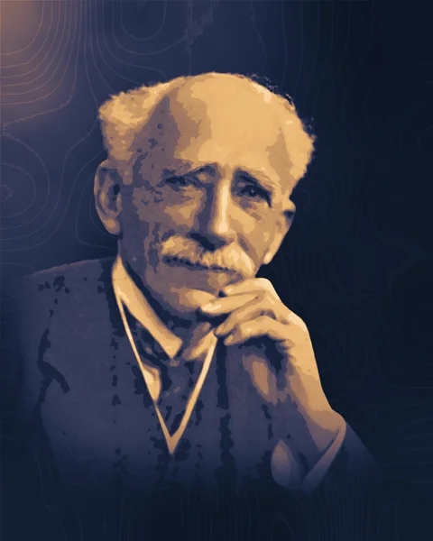
John Ambrose Fleming
1849–1945
He turned a light bulb with an extra plate into the oscillation valve of 1904, a vacuum tube that passes current one way only, which the Computer History Museum calls the first practical electronic device.
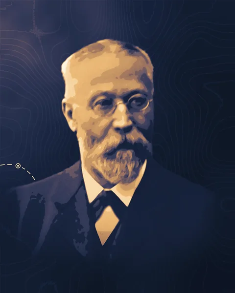
Karl Ferdinand Braun
1850–1918
He found in 1874 that a metal point on a crystal lets current through one way only, the effect behind the semiconductor diode, and in 1897 he built the cathode-ray tube.

Jagadish Chandra Bose
1858–1937
He detected radio waves with a metal point pressed on a crystal in the 1890s and filed the first patent on a semiconductor crystal detector in 1901.
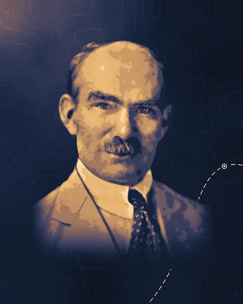
Lee de Forest
1873–1961
He put a third electrode, the grid, into the vacuum tube in 1906 and so made the Audion, the first widely used device that could amplify an electrical signal.
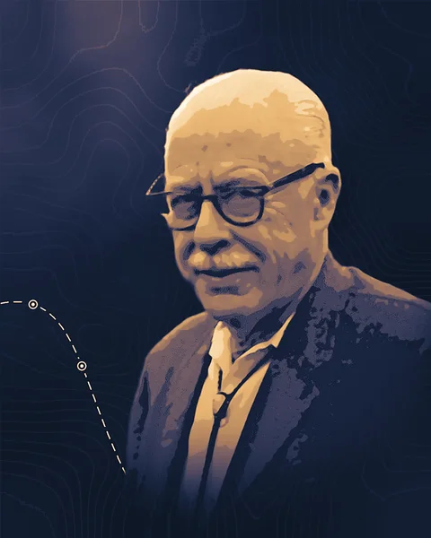
Walter Brattain
1902–1987
He built and ran the experiments that gave the first transistor, made with John Bardeen at Bell Labs in December 1947.
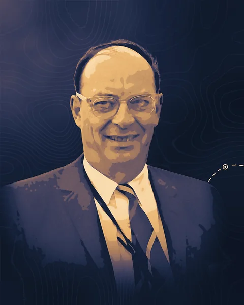
John Bardeen
1908–1991
He worked out why earlier solid amplifiers had failed, and with Walter Brattain made the first transistor at Bell Labs in December 1947.

Morris Chang
born 1931
He founded TSMC as a factory that makes other companies' chips and designs none of its own, which let chip companies exist without a factory.
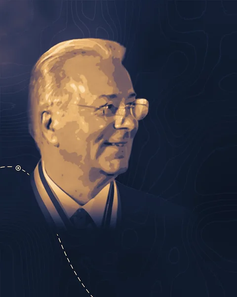
Federico Faggin
born 1941
He made the silicon-gate transistor into a working chip process and used it to design the Intel 4004, the first microprocessor sold.

Chenming Hu
born 1947
He led the Berkeley team that built the FinFET, the fin-shaped transistor in today's advanced chips, and the transistor models that chip designers simulate with.
Advances to build with
2 research notes
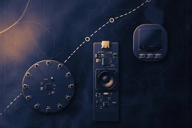
Claude Fable 5.2
Three working devices
Anthropic says its AI model Claude Fable 5.2 designed three prototype devices that worked without electrical modifications, with no outside test reported.

NVIDIA GR00T 2
Five demonstrations per task
By NVIDIA's own test, its robot model GR00T 2 averages 95% success after five demonstrations of a task, on 50 tasks picked from those it learns that way.
Open in electronics and semiconductors
3 of 15 open deliverables
Open · Chip design
Agent-designed tile proven in silicon
Give an AI coding agent a one-page spec for a small block, such as a serial-port transmitter or an 8-bit multiplier, and have it produce a Tiny Tapeout tile (one design slot on a shared community chip) with no human edits to the design, tests or tool settings. Submit it to a shuttle, and when the chips arrive, test them against acceptance tests that a second person wrote beforehand and kept from the agent.
Built with what exists
a coding agent such as Claude Code running an AI model such as Claude Fable 5.2 (the Note "Three working devices" covers the same question for circuit boards); Tiny Tapeout's Verilog template, which builds the layout with the open LibreLane flow and runs a precheck on GitHub; cocotb and Icarus Verilog for tests; a Tiny Tapeout demo board and its MicroPython SDK to test the finished chips.
Open · Wafer fabrication
An open nanosheet transistor
A free, scripted pipeline that builds a three-sheet nanosheet transistor step by step in a process emulator, then computes its current-voltage curves in an open device simulator. A process emulator models how each fab step changes the shape of the structure; a device simulator computes how charge moves through the finished shape.
Built with what exists
ViennaPS (process emulation, Python), DEVSIM (device simulation), Gmsh (meshing), ParaView (viewing), Python, GitHub.
Open · Lithography
Open EUV mask-correction benchmark
A public dataset of at least 10,000 small layout clips from layers printed with EUV, each with its target shape, its simulated print and a reference corrected mask. Mask correction means reshaping the mask so the printed shape comes out right; the simulation should include the way light bounces off a thick EUV mask. Publish baseline models that predict the print and the corrected mask.
Built with what exists
EUVlitho, an open EUV simulator from the Institute of Science Tokyo; the ASAP7 7 nm teaching design kit, which assumes EUV for key layers; OpenROAD to lay out example designs; KLayout to cut clips; PyTorch; LithoBench's code as a template.